Send Simple Ordered with airSlate SignNow
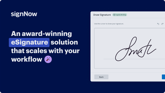
Award-winning eSignature solution


Do more online with a globally-trusted eSignature platform
Standout signing experience
Trusted reporting and analytics
Mobile eSigning in person and remotely
Industry polices and conformity
Send simple ordered, quicker than ever
Helpful eSignature extensions
See airSlate SignNow eSignatures in action


airSlate SignNow solutions for better efficiency
Our user reviews speak for themselves


Why choose airSlate SignNow
-
Free 7-day trial. Choose the plan you need and try it risk-free.
-
Honest pricing for full-featured plans. airSlate SignNow offers subscription plans with no overages or hidden fees at renewal.
-
Enterprise-grade security. airSlate SignNow helps you comply with global security standards.

Your step-by-step guide — send simple ordered
Using airSlate SignNow’s eSignature any business can speed up signature workflows and eSign in real-time, delivering a better experience to customers and employees. send simple ordered in a few simple steps. Our mobile-first apps make working on the go possible, even while offline! Sign documents from anywhere in the world and close deals faster.
Follow the step-by-step guide to send simple ordered:
- Log in to your airSlate SignNow account.
- Locate your document in your folders or upload a new one.
- Open the document and make edits using the Tools menu.
- Drag & drop fillable fields, add text and sign it.
- Add multiple signers using their emails and set the signing order.
- Specify which recipients will get an executed copy.
- Use Advanced Options to limit access to the record and set an expiration date.
- Click Save and Close when completed.
In addition, there are more advanced features available to send simple ordered. Add users to your shared workspace, view teams, and track collaboration. Millions of users across the US and Europe agree that a solution that brings everything together in a single holistic enviroment, is what enterprises need to keep workflows functioning effortlessly. The airSlate SignNow REST API allows you to integrate eSignatures into your app, website, CRM or cloud. Check out airSlate SignNow and enjoy faster, smoother and overall more productive eSignature workflows!
How it works
airSlate SignNow features that users love


Get legally-binding signatures now!
What active users are saying — send simple ordered


Related searches to send simple ordered with airSlate airSlate SignNow

Fax electronically sign ordered
As you probably know, this is a PCB; which stands for printed circuit board. Its job is to basically connect electrical components to one another through the help of copper traces. And I actually showed you in a previous video how I came up with the idea and schematic for this PCB, how I designed it and how I ordered it through a PCB manufacturer. So it pretty much goes without saying that PCBs are often times crucial when it comes to creating your own electrical circuits. Especially if you are dealing with SMD ICs which are so tiny that you can never solder them by hand onto a perfboard and use them. The only downside of such professional PCBs is that it takes at least a week for the PCB manufacturer to produce them and send them to you which is not really ideal when you just want to test out a new design for a specific IC. To bypass this waiting time problem, I tried out PCB etching as well as PCB milling in previous videos which did work to some extent but those methods were definitely not my favourites. That is why I was rather happy when the company Elektor contacted me and sent me over a huge package in which two smaller packages were buried. One of them was the Voltera V-One Desktop PCB Printer and the other one was its fitting Drill Attachment extension. And in this video I will properly test this machine and even create a home-made printed version of one of my older PCB projects in order to find out whether such a printer can replace professional PCB manufacturers. Let's get started! This video is sponsored by Elektor who lent me the PCB Printer showcased in this video to test it out. Since Elektor knows that this product is not affordable for everyone, they kindly offer a 60% discount on an Elektor green membership for one year. With it, you get access to more than 1000 electronics DIY projects and the newest Elektor magazine in digital form every two months. I highly recommend reading them and I even made an appearance in them. First off, I obviously had to unpack all the packages and had a look at not only everything the printer came with but also the printer itself. I have to say that I really do like its all metal design. And while we are talking about good quality, all of the accessories the printer came with all play in this quality region. But that is enough praise for now; let's rather continue by powering the printer, connecting it to my computer, turning it on and browsing through its user manual. There I was guided to the Voltera website on which there were tons of written guides and videos on how to properly use the printer. Even the software later takes you by the hand and not only tells you what steps you have to do next but also shows you how to do them; so there is pretty much no way you can mess something up. But that of course didn't stop me from messing something up but more about that in a second. Before that I installed and opened the software for the printer and then had a look at the two getting started projects on the Voltera website. Now the Hello World project was only single sided and thus did not require drilling; to for example create vias which are kind of mandatory for my own PCB projects. So I skipped that one and instead had a look at the Punk Console which was double sided and comes with vias, perfect. To start this design I added the sacrificial layer for drilling to the bed and clamped the blank PCB in place. Then I clicked the drill icon and loaded the provided Gerber files for the design into the software which then wanted to outline the design size on the blank PCB. For that I added this probe with a long and fine tip to the printer which then did a position calibration through the help of mechanical sensors and then it outlined the size of the design. After I was happy with the position, the printer started measuring the height of different points on the PCB to later create a perfectly flat layer. As soon as that was done I removed the probe head, added the 0.7mm drill bit to the drill head just like the software asked me to do and secured the drill to the printer. After then powering the drill with an extra power supply it was time for drilling and the only thing I can say is that it was super quick. So I pretty much repeated this process once more but this time with a 1.6mm drill which took a bit longer but was still very fast. I then ended the drilling process by vacuuming the work area and cleaning the PCB with isopropanol. Next it was time for printing, for which the software promptly asked me which Ink I wanted to use. My printer came with this one and as you would have guessed the printer basically lays down this ink which will later act just like the copper traces. But anyway after selecting the right one, I chose to reuse the alignment of the drilling and let the printer once again measure the heights on the PCB. After that was done, it was finally time to insert the ink into its dispenser and prime it so that a bit of it comes out of the top. Then I added the dispenser to the printer and let it print a calibration pattern on the PCB. At this point I had to fine adjust the Z height and E factor for the print head which after a few tries delivered pretty decent results. That means it was time for the real ink printing which as you can see in the software did take a couple of minutes but overall there occurred no problems and the result did not look half bad. Next was curing the ink by simply reusing the mounting brackets to hold the flipped board in the air while the bed heated up to 210 degrees Celsius for roughly around one hour. What was weird though was that this process smelled a bit and created fumes which was my mistake though since I apparently ignored the tutorial and forgot to remove the sacrificial layer. But even with this mistake the ink became hard and I was even able to burnish it which is why I continued by printing the bottom side. To get the alignment right we have to position the probe head exactly above two holes on the PCB which was actually quite easy to do. Afterwards the printing process was pretty much the same as with the top layer and once again only the curing took quite a bit of time. And with that being done I successfully printed a double sided PCB which means all that was left to do was to add 0.4mm rivets for the vias and 1.0mm rivets for the through hole components. So I simply pushed those in their designated holes and used the given rivet tools and a hammer to properly secure them all to the board. Next I finally wanted to solder all of the components to the board with the help of the given specialized solder. But as you can see, since I messed up the curing of the top side, the ink simply broke off. The bottom side however accepted the solder without any problems which gave me hope for my home made PCB I wanted to create next. The PCB I want to replicate is this one. It is basically an AC light bulb trailing edge dimmer that I created in a previous video. To start off, I had to remove the big copper area of the original design and had to replace it with some smaller conductor traces. Next I pretty much only had to adjust the hole size for the vias to 0.7mm and the size of the through hole components to 1.6mm. After then exporting the Gerber files and loading them in the Voltera software, it seems like everything should work out just fine. So just like described before I did the drilling, printing the top layer and printing the bottom layer process once again without experiencing any significant problems. Afterwards though I realized that some top layer ink traces were too close to one another. So I simply used an X-Acto knife to trim the ink traces a bit so that there were no shorts. As soon as that was done, I added the rivets to board and used the given solder paste in order to reflow solder the big MOSFETs onto the PCB. Of course you can also use the solder paste with the printer and reflow it with it but I didn't feel like doing that because I love to hand solder my components, which I of course then continued to do so. I have to say that I had to get a bit experimental with the potentiometers and the switch but overall I have to say that soldering to the ink was easy to do. And just like that after 4 hours I got my own home-made PCB which after hooking it up to mains voltage seems to work without any problems, awesome. Now even though my second PCB print worked out smoothly and the software and printer are a joy to work with, I highly doubt that it will be the future of PCB manufacturing. The reasons are simple; not only is the printer very expensive, it also requires consumables which are also quite expensive. And while the ink is highly conductive, it is certainly not as conductive as copper and you should not forget that the ink does not come with a solder mask which can be a problem for certain PCB design. And while all of that sounds rather negative, I want to end this video by saying that I think that this printer can be really useful for universities or companies that want to prototype and test out a new PCB design in just a couple of hours. But for me who just creates silly YouTube videos the printer is a tad too expensive which is why I will return it to Elektor now. But everyone who would like to get more information about the Voltera PCB printer can check out the Elektor link in the video description. Anyway I hope you enjoyed this video, if so don't forget to like, share, subscribe and hit the notification bell. Stay creative and I will see you next time.
Show moreFrequently asked questions
How do I sign PDF files online?
How can I make a PDF easy to sign?
How do I sign documents in PDF format?
Get more for send simple ordered with airSlate SignNow
- Decline autograph Catering Proposal Template
- Notarize signature service Camper Health History
- Upload signature block Summer Camp Evaluation
- Create electronic signature Assignment of Partnership Interest
- State byline Deposit Receipt
- Accredit electronic signature 30 day Notice to Landlord
- Warrant countersignature Mobile App Development Proposal
- Ask esigning Benefit Plan
- Propose signed electronically invoice
- Ask for sign Student Trip Planning
- Merge Patient Intake Form countersign
- Rename Subcontractor Agreement Template sign
- Populate NonProfit Donation Consent electronically signing
- Boost Billing Invoice eSign
- Underwrite Hospital Discharge eSignature
- Insure Proforma Invoice Template autograph
- Instruct Photography Proposal Template electronic signature
- Insist CCW Certificate signed electronically
- Order draft electronically sign
- Integrate recipient radio
- Verify subscriber dropdown
- Ink spectator checkbox
- Recommend Restaurant Business Plan Template template signatory
- Size Summer Camp Permission Slip template initials
- Display Formal Letter Template template eSign
- Inscribe Stock Certificate template esigning
- Strengthen Investor Rights Agreement template digisign
- Build up Musical Ticket template electronic signature